ZXCT1032
Issue 4 - June 2007
6
www.zetex.com
?Zetex Semiconductors plc 2007
Application information
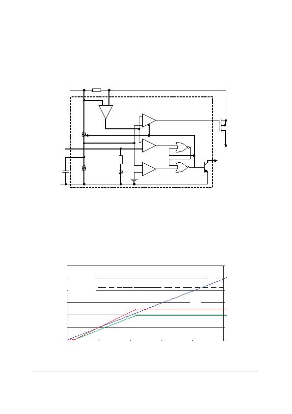
ZXCT1032 block diagram and description
Operation of the ZXCT1032
1 After power-up, the timing capacitor (C
T
) is charged up by a 200礎 current source. This causes
the output amplifier's drive pin to fall in voltage, progressively turning on the PMOS transistor.
The load current is monitored by the current monitor and the amplifier control loop controls
the load current allowing it to increase gradually (soft-start mode) as the voltage on C
T
increases. During the soft-start phase the load current will start to build up while there is a
large voltage across the pass MOSFET; this can lead to large power dissipation if large
capacitive loads are driven and/or large C
T
is used.
ZXCT1032
Load
Flag
Drive
IN+
IN-
T
C
T
GND
I
SET
200A
3.3A
2.1V
80mV
1
(2)
(3)
(4)
(5)
(6)
(8)
R
SENSE
I
CT-CHG
I
CT DIS
50k
-
-
+
+
+
+
-
-
-
-
ZXCT1032 Start up characteristic
0
0.5
1
1.5
2
2.5
3
0
0.5
1
1.5
2
2.5
im - m
0
0.2
0.4
0.6
0.8
1
1.2
V
ISET
V
CT
10*V
SENSE
I
LOAD
V
IN+
= 18V
R
SENSE
= 0.2
C
T
= 220nF
V
ISET
= 2.1V
Trip current = 1A
发布紧急采购,3分钟左右您将得到回复。
相关PDF资料
ZXCT1041E5TA
IC CURRENT MONITOR 1% SOT23-5
ZXCT1050E5TA
IC CURRENT MONITOR 3% SOT23-5
ZXCT1051E5TA
IC CURRENT MONITOR 1% SOT23-5
ZXCT1080E5TA
IC CURRENT MONITOR 3% SOT23-5
ZXCT1081E5TA
IC CURRENT MONITOR 3% SOT23-5
ZXCT1085E5TA
IC CURRENT MONITOR 3% SOT23-5
001-0001
ANTENNA 2.4GHZ DIPOLE 2DBI
001-0002
ANTENNA 900MHZ DIPOLE 2DBI
相关代理商/技术参数
ZXCT1032N8TA-CUT TAPE
制造商:DIODES 功能描述:ZXCT1032 Series 2.5 uA 9.5 to 21 V Controller and Electronic Fuse - SOIC-8
ZXCT1041
制造商:ZETEX 制造商全称:ZETEX 功能描述:Bidirectional precision high-side current monitor
ZXCT1041E5TA
功能描述:电流和电力监控器、调节器 Bi-Direct High Side RoHS:否 制造商:STMicroelectronics 产品:Current Regulators 电源电压-最大:48 V 电源电压-最小:5.5 V 工作温度范围:- 40 C to + 150 C 安装风格:SMD/SMT 封装 / 箱体:HPSO-8 封装:Reel
ZXCT1050
制造商:DIODES 制造商全称:Diodes Incorporated 功能描述:Precision wide input range current monitor
ZXCT1050E5TA
功能描述:电流和电力监控器、调节器 Wide CMR Curr. Mon. RoHS:否 制造商:STMicroelectronics 产品:Current Regulators 电源电压-最大:48 V 电源电压-最小:5.5 V 工作温度范围:- 40 C to + 150 C 安装风格:SMD/SMT 封装 / 箱体:HPSO-8 封装:Reel
ZXCT1051
制造商:ZETEX 制造商全称:ZETEX 功能描述:Precision wide input range current monitor
ZXCT1051_0611
制造商:ZETEX 制造商全称:ZETEX 功能描述:Precision wide input range current monitor
ZXCT1051E5TA
功能描述:电流和电力监控器、调节器 Precision Wide Input RoHS:否 制造商:STMicroelectronics 产品:Current Regulators 电源电压-最大:48 V 电源电压-最小:5.5 V 工作温度范围:- 40 C to + 150 C 安装风格:SMD/SMT 封装 / 箱体:HPSO-8 封装:Reel
